
Termination in High Frequency PCB Layouts
As the use of electronic devices grows, so does the demand for higher transmission frequencies to accommodate the increased data rates. High-speed PCBs are used in a wide variety of applications, including mobile telephone base stations, satellite systems and data communication. In order to meet the demands of high-speed signals, designers must employ strict design techniques and precise layout guidelines to avoid impedance mismatches and other issues that can cause signal loss, crosstalk, reflections and ground bounce.
One of the most important aspects of high-frequency PCBs is impedance matching, which minimizes signal reflections at interconnects. This involves carefully designing trace widths, spacing and stack-up configurations to ensure consistent impedance along transmission lines. It is also vital to reduce the number of vias in a circuit board because they can introduce unwanted inductance and capacitance effects.
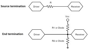
Signal termination is another crucial element of high frequency pcb because it allows for proper decoupling of signal lines from power and ground planes. Without adequate termination, signal currents may flow across the surface of the PCB and induce a voltage spike called crosstalk that can interfere with adjacent lines and create data errors. It is also important to avoid shorts between traces and the ground plane because they can reduce signal transmission speed, generate heat and cause damage.
The Role of Signal Termination in High Frequency PCB Layouts
Several factors can affect the impedance of high-speed transmission lines, including line thickness, dielectric constant, and the distance between the line and the ground plane. To mitigate these issues, designers can implement a number of techniques, including differential signaling, use of decoupling capacitors and stackup design. Additionally, careful consideration should be given to the placement of power and ground planes and implementing the 20H rule to reduce plane coupling.
High-speed signal transmission is a critical aspect of many applications, including the Internet of Things (IoT), smart cars and smartphones. However, it can be difficult to achieve the desired performance in a small footprint due to limited space on a PCB. To address these challenges, designers can use several techniques to improve signal integrity, such as using differential signaling, reducing the thickness of traces and using appropriate layout techniques.
Another factor that influences signal performance is the presence of EMI interference. This can be caused by the fast switching of signals that induces voltage spikes in neighboring traces, resulting in crosstalk and reflections. It can also be caused by power noise or electromagnetic interference from external sources. To minimize these interferences, designers can utilize shielding techniques and follow best practices for laying out the PCB.
High-speed PCBs can be difficult to fabricate because they require precise layer thicknesses, tight tolerances and accurate positioning of components. In addition, the material selection must be chosen carefully to maintain a high-performance system at a low cost. To address these issues, engineers can use hybrid designs where they use expensive materials in areas of the PCB that are most impacted by high-speed signals. This can help them keep the cost down while still ensuring the quality and reliability of the final product.
